SiS 85C471
Chipset part
1039
Empty
Description:
Introduction
The SiS85C471 is a high performance, 100% PC/AT compatible single chip controller, designed for cached/non-cached P24D/P24T/P24C, M6/M7 or 486 PC systems. The high integration of the powerful cache controller, the DRAM controller, the CPU interfaces, the bus controller, the data buffers and the peripheral controllers provides an easy and economical solution for compact board manufacturing.
Features
- 208-Pin Perpendicular Quad Flat Package (PQFP)
- 0.8μm Low Power CMOS Technology
- Fully IBM PC/AT Compatible. 80486DX2/DX/SX/SL Enhanced, P24D/P24T/P24C, M6/M7 and Am486DXL/Am486DXL2 Single Chip Controller
- Supports L1 Cache Write back CPU (P24T/P24D/M6/M7) systems
- Direct Mapped Cache Controller
- Write-Back or Write-Through Schemes
- Bank Interleave or Non-Interleave Cache
- 0/1 Wait State Cache Write Hit
- Flexible Cache Size : 32/64/128/256/512KB or 1MB
- 7 bits or 8 bits TAG addresses
- Flexible 2-1-1-1, 3-1-1-1, 2-2-2-2 and 3-2-2-2 Burst Read/Write Timing
- Fast Page Burst Mode DRAM Controller
- 4 Banks up to 128MB of DRAMs
- 256K/512K/1M/2M/4M/16MxN DRAM Type
- Programmable DRAM Speed
- Double-sided SIMMs
- Two Programmable Non-Cacheable Regions (64KB-4MB area)
- CAS before RAS Transparent DRAM Refresh
- BIOS/Video ROM Cacheable
- Shadow RAM in Increments of 32KB
- Option to Disable Cache in Shadow RAM Area
- 256K Memory Relocation
- 8042 Emulation of Fast A20GATE and CPU Reset
- Supports Port 92h
- Hardware/Software De-Turbo Switch
- Supports Two VL-Bus Master
- Supports Flash Memory
- Supports Double/Single frequency input
- CPU Operating frequency 0-100 MHz
- Supports Power Management Mode
- Supports the SMM and the SMI
- CPU Stop Clock Function
- Four Power Saving States
- Long and Short System Timers
- Supports the APM control
- Supports Break Switch control
- Power Saving also on non-SMI CPU
- More System Event Monitoring and the Power Saving Control
- AT Bus State Machine and Controller
- Synchronous/Asynchronous AT Bus Clock
- Programmable AT Bus Speed
- 1/2,1/3,1/4,1/5,1/6,1/8,1/10 of Input Clock or 7.159MHz
- Programmable Wait State Generation
- 1 or 2 Wait States for 16-Bit Transfers
- 4 or 5 Wait States for 8-Bit Transfers
- Programmable I/O Recovery Time
- Programmable driving current for the DRAM and the ISA bus signals
- 32-Bit Data Buffer Between CPU and AT System
- Data Conversion and Swapping Logic for 32-/16-/8-Bit Transfers During CPU and DMA Cycles
- Data Latches for AT Read Cycles
- Parity Generation and Detection Logic
- Port B Register and NMI Logic
- Integrated Peripheral Controllers
- 8259Ax2 / 8237x2 / 8254 / 74LS612
- 387/487SX and Weitek 3167/4167 Coprocessors Interface
Last updated 2019-04-30T00:00:00Z
No chip specs
Release date
File
Logs
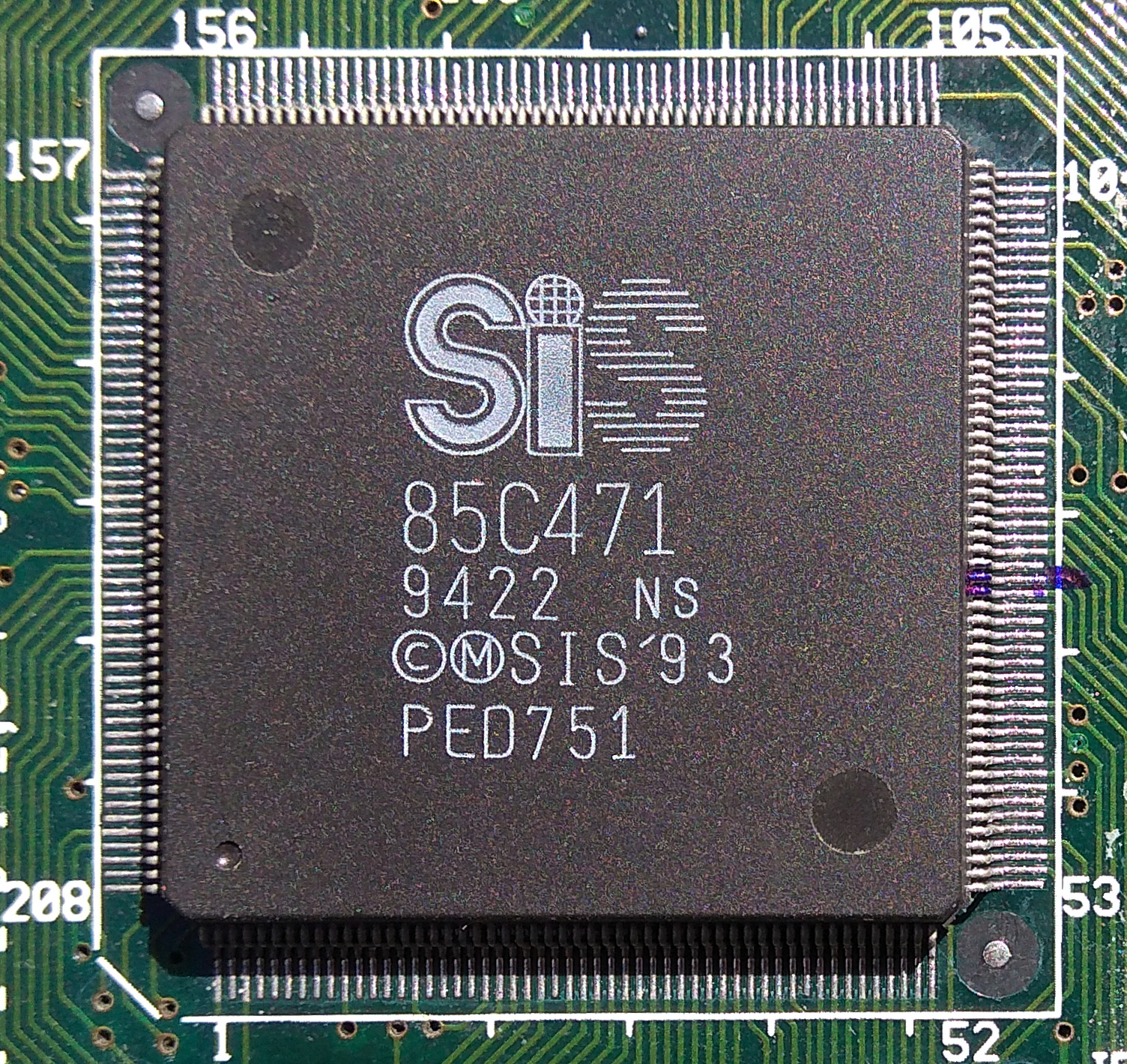 Image 1 of 1 (Rigo "0xCats" Reddig)
Disclaimer
The info found in this page might not be entirely correct. Check out this guide to learn how you can improve it.