Description:
The 82437MX Mobile System Controller (MTSC) integrates the cache and main memory DRAM control functions and provides bus control for transfers between the CPU, cache, main memory, and the PCI Bus. The second level (L2) cache controller supports a write-back cache policy for cache sizes of 256 Kbytes and 512 Kbytes. Cacheless designs are also supported. The cache memory can be implemented with either standard, burst, or pipelined burst SRAMs. An external Tag RAM is used for the address tag and an internal Tag RAM for the cache line status bits. For the MTSC DRAM controller, four rows are supported for up to 128 Mbytes of main memory. The MTSC optimized PCI interface allows the CPU to sustain the highest possible bandwidth to the graphics frame buffer at all frequencies. Using the snoop ahead feature, the MTSC allows PCI masters to achieve full PCI bandwidth.
■ Integrated Second Level Cache Controller
- Direct Mapped Organization
- Write-Back Cache Policy
- Cacheless, 256 Kbytes, and 512 Kbytes
- Standard, Burst and Pipelined Burst SRAMs
- Cache Hit Read/Write Cycle Timings at 3-1-1-1 with Burst or Pipelined Burst SRAMs
- Back-to-Back Read Cycles at 3-1-1-1-1-1-1-1 with Burst or Pipelined Burst SRAMs
- Integrated Tag/Valid Status Bits for Cost Savings and Performance
- Supports 3.3 V SRAMs and Tag Address
■ Integrated DRAM Controller
- 64-Bit Data Path to Memory
- 4-Mbyte to 128-Mbytes Main Memory
- EDO/Hyper Page Mode DRAM (x-2-2-2 Reads) Provides Superior Cacheless Designs
- Standard Page Mode DRAMs
- 4 RAS Lines
- 4 Qword Deep Buffer for 3-1-1-1 Posted Write Cycles
- Symmetrical and Asymmetrical DRAMs
- 3 V or 5 V DRAMs
■ Fully Synchronous 25/30/33 MHz PCI Bus Interface
- 100 Mbytes/s Instant Access Enables Native Signal Processing on Pentium Processors
- Synchronized CPU-to-PCI Interface for High Performance Graphics
- PCI Bus Arbiter: MPIIX and Three PCI Bus Masters Supported
- CPU-to-PCI Memory Write Posting with 4 Dword Deep Buffers
- Converts Back-to-Back Sequential CPU to PCI Memory Writes to PCI Burst Writes
- PCI-to-DRAM Posting of 12 Dwords
- PCI-to-DRAM up to 120 Mbytes/s Bandwidth Utilizing Snoop Ahead Feature
■ Power Management
- DRAM Refresh During Suspend
- Self Refresh and Extended Refresh
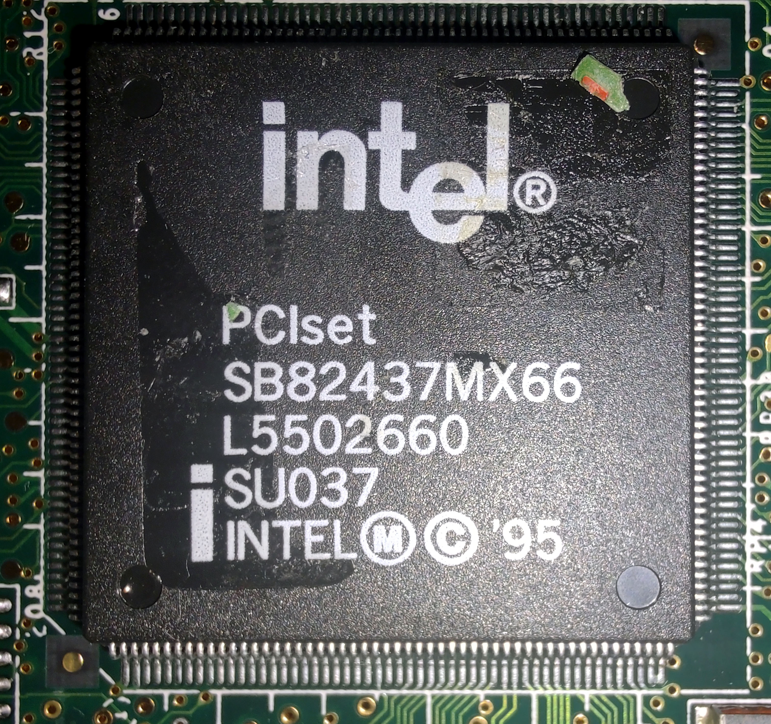 Image 1 of 1 (bjwil1991 (retro-pc_user))
Disclaimer
The info found in this page might not be entirely correct. Check out this guide to learn how you can improve it.